ARCTURUS

    ALPHA ABOUT MEDIA BLOG OMEGA
  1. AIRCRAFT
  2. AUTO
  3. CAMERA
  4. COMPUTER
  5. IPHONE
  6. ROBOTICS
  7. SATELLITES
  8. SEMICONDUCTOR
  9. SUBMARINE
  10. TECHNOLOGY
SEMICONDUCTORS
A microchip.


Semiconductors are fundamental to nearly all modern industrial and national security activities, and they are essential building blocks of current and emerging technologies, such as artificial intelligence, autonomous systems, next generation communications, and quantum computing.


SEARCH: LIBRARY of CONGRESS SUBJECT HEADINGS
A microchhip diagram.
TECHNOLOGY - T
  • Subclass TK452 - 454.4: Electric networks.
  • Semiconductors - ASML
  • Semiconductors - TSMC
  • Semiconductors - Production
  • Semiconductors - Wire bonding
  • Semiconductors - Silicon Wafers
  • Semiconductors - Manufacturing
  • Semiconductors - Supply Shortage
  • Semiconductors - Structural analysis
  • Semiconductors - ASML / TSMC / INTEL
  • Semiconductors - Product development
  • Semiconductors - Microchip processing
  • Semiconductors - Materials engineering
  • Semiconductors - Digital analysis / design
  • Semiconductors - Silicon wafer transistion
  • Semiconductors - Factory Architectural Design Plan


SUBJECT EXPERTS I
SUBJECT EXPERTS II

RESEARCH GUIDES

SEMICONDUCTOR NEWS
Program Development

Since no region has end-to-end capabilities for semiconductor design / microchip design and manufacturing, program development is restricted to a particular niche within the field. A business—or even a group of businesses within a region—may become a center(s) of expertise.

Design Aspects

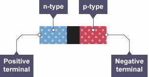
Integrated circuit design involves the creation of electronic components: transistors, resistors, capacitorsand the interconnection of these components onto a piece of microchip, typically silicon or other pure elements. Microchips are created by adding impurities to the element.

Design Constraints

Developing semiconductor chips involves several key procedures that must be addressed such as product definition, design options, schedule and cost. Many tech companies have begun developing their own chips and that will likely help the industry in the future.

Design Optimization

Semiconductor manufacturing projects require the expertise of research/development personnel to initiate the automation process. Once the process is engaged, the technical aspects of implementation are supervised by different teams comprised of mechanical / electrical / engineers along with technicians to assure synchronization of the processes.

Designing Semiconductors

Computer software development tools can create optimal semiconductor designs consisting of layouts with specifications along with annotated peripherals. Engineers can use the software for co-operating during the design procedure, pulling old designs of circuit board components from libraries of printed circuit boards (PCB) and verify schematic diagrams of circuits.

Design Process/Simulation

Microchip process simulation is the modeling of the fabrication of semiconductor devices such as transistors. It is a branch of electronic design automation, and part of a sub-field known as technology CAD, or TCAD. Process simulation deals with modeling the fabrication on front end of line manufacturing steps. Back-end-of-line steps use tools like Sentaurus Interconnect.

ASCEND

SEMICONDUCTORS 2024

Everyone in the semiconductor industry, everyone in the technology industry, would benefit from more diversity in the business.

- Lisa Su -: 1969 AZ Quotes
A microchip symbol.


Designing a Semiconductor Facility

In the microelectronics industry, a semiconductor fabrication plant (commonly called a fab; sometimes foundry) is a factory where devices such as integrated circuits are manufactured. Fabs require many expensive devices to function. Estimates put the cost of building a new fab over one billion U.S. dollars with values as high as $3 to 4 billion not being uncommon. Taiwan Semiconductor Manufacturing Company {TSMC} invested $9.3 billion in its Fab15 300 mm wafer manufacturing facility in Taiwan. The same company estimations suggest that their future fab might cost $20 billion. Thus, a business model emerges in 1990s, so called foundry model, that operates for the purpose of fabricating the designs of other companies, such as fabless semiconductor companies, is known as a semiconductor fab, or a foundry. If a foundry does not also produce its own designs, it is known as a pure-play semiconductor foundry. When a foundry produces its own designs, it is known as an integrated device manufacturer (IDM).

The central part of a fab is the clean room, an area where the environment is controlled to eliminate all dust, since even a single speck can ruin a microcircuit, which has nanoscale features much smaller than dust particles. The clean room must also be damped against vibration to enable nanometer-scale alignment of machines and must be kept within narrow bands of temperature and humidity. Vibration control may be achieved by using deep piles in the cleanroom's foundation that anchor the cleanroom to the bedrock, careful selection of the construction site, and/or using vibration dampers. Controlling temperature and humidity is critical for minimizing static electricity. Corona discharge sources can also be used to reduce static electricity. Often, a fab will be constructed in the following manner: (from top to bottom): the roof, which may contain air handling equipment that draws, purifies and cools outside air, an air plenum for distributing the air to several floor-mounted fan filter units, which are also part of the cleanroom's ceiling, the cleanroom itself, which may or may not have more than one story, a return air plenum, the clean subfab that may contain support equipment for the machines in the cleanroom such as chemical delivery, purification, recycling and destruction systems, and the ground floor, that may contain electrical equipment. Fabs also often have some office space.

Physical chip model.

The clean room is where all fabrication takes place and contains the machinery for integrated circuit production such as steppers and/or scanners for photolithography, in addition to etching, cleaning, doping and dicing machines. All these devices are extremely precise and thus extremely expensive. Prices for most common pieces of equipment for the processing of 300 mm wafers range from $700,000 to upwards of $4,000,000 each with a few pieces of equipment reaching as high as $130,000,000 each (e.g. Extreme Ultraviolet (EUV) scanners). A typical fab will have several hundred equipment items.

There has been a trend to produce ever larger wafers, so each process step is being performed on more and more chips at once. The goal is to spread production costs (chemicals, fab time) over a larger number of saleable chips. It is impossible (or at least impracticable) to retrofit machinery to handle larger wafers. This is not to say that foundries using smaller wafers are necessarily obsolete; older foundries can be cheaper to operate, have higher yields for simple chips and still be productive. The industry was aiming to move from the state-of-the-art wafer size 300 mm (12 in) to 450 mm by 2018. As of July 2022, Intel has not moved to 450 mm deployment. It must be noted that in 2016, corresponding joint research efforts were stopped. Additionally, there is a large push to completely automate the production of semiconductor chips from beginning to end. This is often referred to as the "lights-out fab" concept.

The International Sematech Manufacturing Initiative(ISMI), an extension of the US consortium SEMATECH, is sponsoring the "300 mm Prime" initiative. An important goal of this initiative is to enable fabs to produce greater quantities of smaller chips as a response to shorter lifecycles seen in consumer electronics. The logic is that such a fab can produce smaller lots more easily and can efficiently switch its production to supply chips for a variety of new electronic devices. Another important goal is to reduce the waiting time between processing steps.

Physical chip model.
ASCEND

Foundries and Assembly Houses

Emerging semiconductor companies must look for new competitive edge whether its price, performance, or power consumption. There is a lot to gain in the production phase if a startup can gain advantages in the aforementioned areas. New technologies in packaging can reduce the total device cost and better collaboration with a foundry can give the new semiconductor company a better understanding on how to optimize its design for better performance. On the other hand, assembly house and foundries are looking for new requirements in order to drive new products and technologies and without having direct contact to the market they are missing real-life demands to enable new features.

• Integrated Device Manufacturers (IDMs).

An IDM is a semiconductor company which designs, manufactures, and sells integrated circuit (IC) products. Due to the dynamic nature of the semiconductor industry, the term IDM has become less accurate than when it was coined. While Qualcomm, Broadcom and other large IDMs are looking for getting more market share and beat competition maybe you can help them. By using IDMs distribution channels you can get closer to your customers and even more close to get some cash. The difficult part is to find the IDMs can use teh technology of emerging semiconductor companies immediately. Startups should connect to the IDMs business development offices to see if their offerings are compatible with their sales strategy. There have been several start-up and IDMs engagement in the past that resulted in a mutually beneficial relationships.

• Semiconductor Suppliers

To lower the risk and reduce time to market, an emerging semiconductor company needs reliable business associates. Use the {AnySilicon }search tool to identify vendors that can support you quickly. Some suppliers offer very professional solutions and services together with creative business models that can help with reducing the upfront investment. A combination of technical and commercial engagement could be a key to the success and really add value for an emerging semiconductor company.

• Consultative Design

One of the greatest errors concerns product definition. Engineers and managers believe they know what customers want even without meeting them or talking to them. In any company, and especially in hardware-based companies, where there is a lot of money involved with product re-definition and changing a product can be expensive. For fabless companies adding a feature which is hardware-related as opposed to software related can also increase expenditures. Adding functionality into the silicon will consist of: design and verification of the Application Specific Intergrated Circuit (ASIC), a new maskset, production test updates and sometimes changing the package type. This requires a huge capital investment and at least 6-12 months of delay.

• An Innovative Approach

There are many examples of fabless companies changing their business models and ending up selling a product instead of a chip. The motivation behind this step was mostly because they could not find any customers for their silicon — so they decided to design, build and sell the end-product themselves. There are great examples of chip companies selling end products. SanDisk is one of them. It is known as the Universal Serial Bus (USB) - stick company, but actually the core competence of the company is the production of the application specific intergrated circuit. The end product is different and obviously generate much more profit. This means that Instead of selling chips, a company may want to think vertical – can they sell an entire product based on its chip or perhaps a module?

• Purchase Intellectual Properties (IPs)

In electronic design, a semiconductor intellectual property core (SIP core), IP core, or IP block is a reusable unit of logic, cell, or integrated circuit layout design that is the intellectual property of one party. The term comes from the licensing of the patent or source code copyright that exists in the design.

Finally, for any semiconductor startup it is easier to purchase IP blocks than to develop them. Listings are located at: AnySilicon, Chip Estimate, Design and Utilization.

ORGANIC SEMICONDUCTORS
ISRAEL: A SEMICONDUCTOR SUCCESS
INDIA'S FAILED SEMICONDUCTOR INDUSTRY
A Microchip Facility.
A world map in black and white ASCEND

Copyright© 2090 / RENAISSANCE RESEARCH /